NVIDIA GeForce 7800 GTX
Architectural Overview & Key Features
![]()
;) The GPU codenamed G70 at the heart of the GeForce 7800 GTX is an incredibly complex chip. If you remember, the NV40 (GeForce 6800 Ultra) comprises over 222 million transistors, which was considered huge at the time of its launch. But with the G70, NVIDIA has taken things a step further. According to NVIDIA, the G70 is made up of over 302 million transistors, an increase of about 80 million. With a chip this complex, NVIDIA was quick to point out that the G70 has more transistors than the number that comprise the XBox GPU (60 million), a PS2 Graphics Synthesizer (43 million), a Game Cube Flipper (51 million), a Game Cube Gekko (21 million), an XBox Pentium III CPU (9 million), a PS2 Emotion Engine (10.5 million), and an Athlon FX 55 (105.9 million) combined.
The GPU codenamed G70 at the heart of the GeForce 7800 GTX is an incredibly complex chip. If you remember, the NV40 (GeForce 6800 Ultra) comprises over 222 million transistors, which was considered huge at the time of its launch. But with the G70, NVIDIA has taken things a step further. According to NVIDIA, the G70 is made up of over 302 million transistors, an increase of about 80 million. With a chip this complex, NVIDIA was quick to point out that the G70 has more transistors than the number that comprise the XBox GPU (60 million), a PS2 Graphics Synthesizer (43 million), a Game Cube Flipper (51 million), a Game Cube Gekko (21 million), an XBox Pentium III CPU (9 million), a PS2 Emotion Engine (10.5 million), and an Athlon FX 55 (105.9 million) combined.
The G70 is a native PCI Express chip, that's produced at TSMC on the fab's .11 micron manufacturing line; while the NV40 is produced on TSMC's .13 micron line. Moving to the more advanced .11 micron process gives NVIDIA the ability to produce more die per wafer than they would have been able to on the .13 micron line (given the chip's overall significantly increased transistor count), so the G70 shouldn't be all that much more expensive to produce than the NV40, even though it's a more complex chip.
On a side note, you may be wondering where the G70 codename came from after years of NVxx codenames. Well, it was simply an engineering decision that made it easier for NVIDIA to track products and designs. And no, the G70 is not a re-named NV47 according to NVIDIA. The NV47 project was terminated and NVIDIA moved onto a next-generation chip because of the timing of tapeouts and their engineering team's ability to deliver a more powerful chip.
|
G70 Architecture Block Diagram
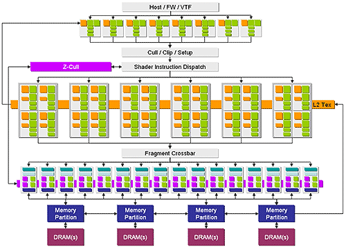
The high-level diagram of the GeForce 7800 GTX architecture reveals three of the major differences between it and a GeForce 6800 Ultra. As you can see, the GeForce 7800 GTX has eight vertex shaders, versus six for a GeForce 6800 Ultra. And the 7800 GTX is equipped with 24 pixel shader-pipelines - 50% more than the GeForce 6800 Ultra, which has 16. Also note that the GeForce 7800 GTX has 16 ROPs (Render Operators) to compliment the 24 pixel shaders; it's not a 1:1 configuration like the NV40. Having more vertex shaders and 1.5x the number of pixel shaders alone would have been enough to make the GeForce 7800 GTX much faster than a GeForce 6800 Ultra, clock-for-clock, but a high-level diagram does not tell the whole story. We've got to dig in a bit further for that...
 Close Up: GeForce 7800 GTX Vertex Shader |
 Close Up: GeForce 7800 GTX Pixel Shader |
NVIDIA had stated that the GeForce 7800 GTX's GPU pipelines have been completely re-architected, and as such this GPU should be considered a brand-new Shader Model 3 architecture. Apparently NVIDIA analyzed over 1300 shaders used in today's more popular applications, and based on their findings they tweaked the 7800 GTX's shaders to remove or reduce as many potential bottlenecks as possible. The end result was a GPU with individual pipelines that are up to 50% more efficient clock-for-clock, that can do far more math per pixel than a GeForce 6800 Ultra in any given timeframe. And as you'll see later, the architectural improvements found in the GeForce 7800 GTX translate into significant real-world performance gains.
Other tweaks deep within the pipeline:
There are also a few other low-level pipeline improvements incorporated throughout the G70. For example, the GeForce 7800 GTX's texture fetch efficiency has been improved significantly, especially for large textures, and efficiency of Cull and Setup operations has been improved by over 30% versus the 6800 Ultra in fixed-function portions of the geometry pipeline. Rotated-Grid anti-aliasing performance has also been improved, as has filtering performance. And perhaps, best of all, the GeForce 7800 GTX was designed with power efficiency in mind. Even though the G70 is comprised of 80 million more transistors, and is clocked higher than a GeForce 6800 Ultra (430MHz vs. 400MHz/425MHz), the GeForce 7800 GTX's peak power utilization is reportedly lower than a 6800 Ultra. NVIDIA claims the GeForce 7800 GTX draws a maximum of 100-110 watts versus 110-120 watts for a 6800 Ultra.


