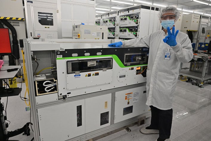
Intel Tech Tour Malaysia: Behind The Scenes Of Cutting-Edge Chip Manufacturing
Intel's Penang Assembly & Testing Operations Unveiled
Assembling Chips With Advanced Packaging Techniques
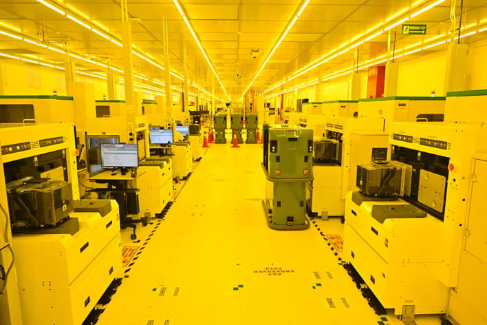
From there, reels are sent to Intel’s Assembly and Test facilities around the globe. One of these facilities resides back in Penang, known as PGAT, located at building PG8. The process here begins where Die Sort Die Prep left off, with reels of dies ready to be assembled with advanced packaging into finished products.
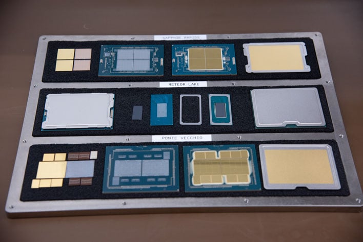
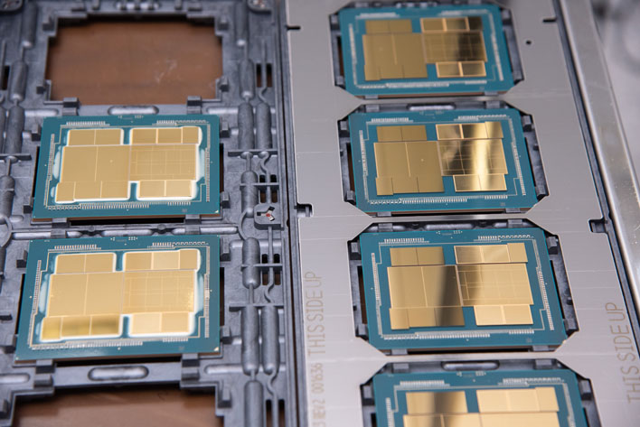
The high-level overview is that the dies are aligned and stacked, then an epoxy underfill is applied and cured before the integrated heat spreader (IHS) is put in place with thermal interface material (TIM) and adhesive. We mostly watched this process for Intel’s Sapphire Rapids CPU and Ponte Vecchio GPU products. Not only is the facility handling more than just CPUs, but it is combining silicon from its own fabs with tiles fabbed elsewhere, like TSMC.
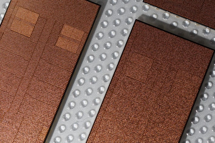
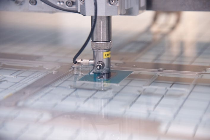
The Chip Attach process begins with flip-chip packaging to get the components in place on a substrate. Each chip has hundreds or thousands of near-microscopic solder balls applied to its surface, which mate with the next chip or substrate layer. The die-to-die multidimensional bonding is Intel’s Foveros advanced packaging technology, first introduced with Lakefield. Intel’s tooling uses a series of vacuums to ensure the dies are applied perfectly flat, as curvature (through thermal warping or mechanical stress) could negatively impact the ability for these solder points to fuse.
Once affixed, there is a miniscule air gap between layers. Intel applies an epoxy underfill to improve stability, ensuring that stresses are distributed evenly across the die. As with the dual saw blades during singulation, Intel can now use two epoxy dispensing nozzles here to improve throughput. There’s no need for suction or anything else, Intel says that capillary action is all that’s needed for it to flow. The chips are later scanned non-invasively (e.g. X-Ray or ultrasound) to ensure there are not any unacceptable voids in the epoxy fill. Some of the epoxy will flow beyond the chip, but this is generally acceptable within reason.
The package is now ready to have the IHS installed. Each chip design has a particular TIM (Thermal Interface Material) that is used, and the machinery dispenses it in a particular pattern to maximize its effectiveness, while balancing other factors like cost. The adhesive for the IHS is dispensed in sequence, and then the IHS lid is finally put in place and cured.
Burn-In And Testing Of Newly Packaged Chips
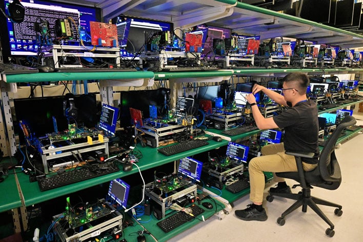
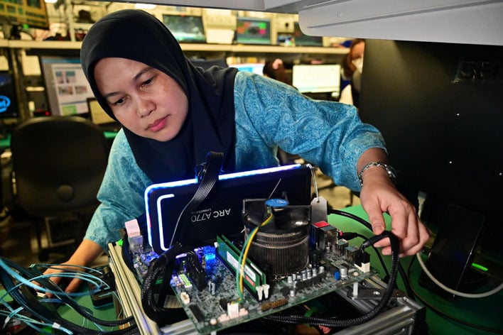
While the manufacturing quality is closely monitored throughout the cycle, Intel conducts final burn-in and testing on each process it manufactures. We got a good look at various stages of testing in the Design And Development Lab at PG16 in Penang. This lab consists of row after row of shelves stuffed full of test equipment to probe every aspect of a product.
The burn-in process is up first, whereby Intel subjects the chips to high temperatures and voltages to screen out defects. Both of these factors are likely the primary killers of CPUs, so each product needs to withstand whatever the end user could throw at it. Chips that survive this process then undergo complete electrical testing where Intel verifies that all traces and other aspects are functioning as intended.
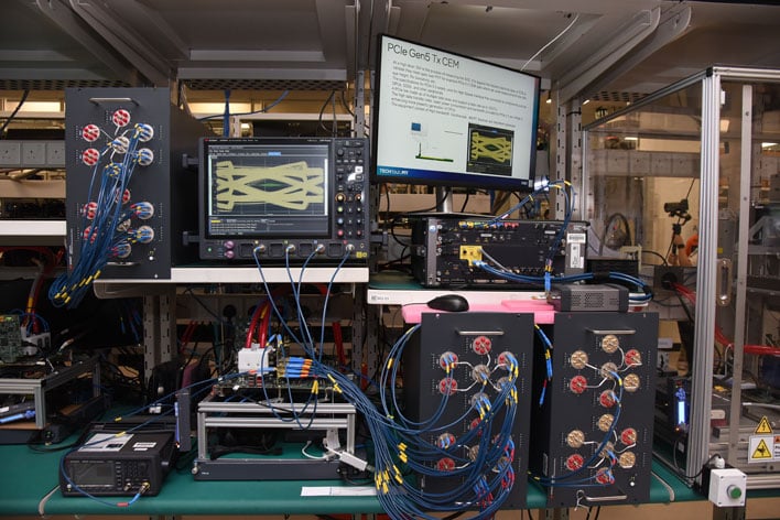
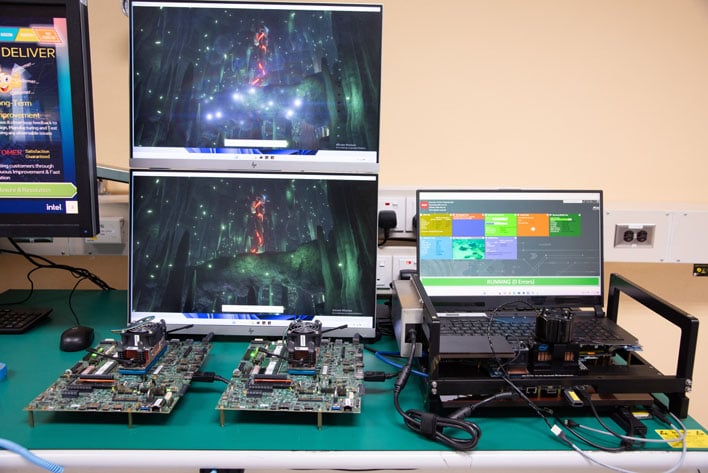
Testing still isn’t complete at this point, though. Intel then loads up each chip into a test environment that mimics a customer environment. This ensures functionality with a range of operating systems and various platform requirements. This is where aspects like memory, PCIe lanes, and other off-chip systems are evaluated.
Building Intel Test Equipment In-House
Near the end of our tour, we got to see where and how some of Intel’s custom test equipment is made. The Intel System Integration and Manufacturing Services (SIMS) facility in Kulim is responsible for making the vast majority of its equipment used to test and validate silicon. The test equipment is then distributed to wherever it is needed at Intel’s facilities around the globe. Internally developed and produced test equipment is vital for Intel to maintain control over the secretive aspects of its manufacturing processes.
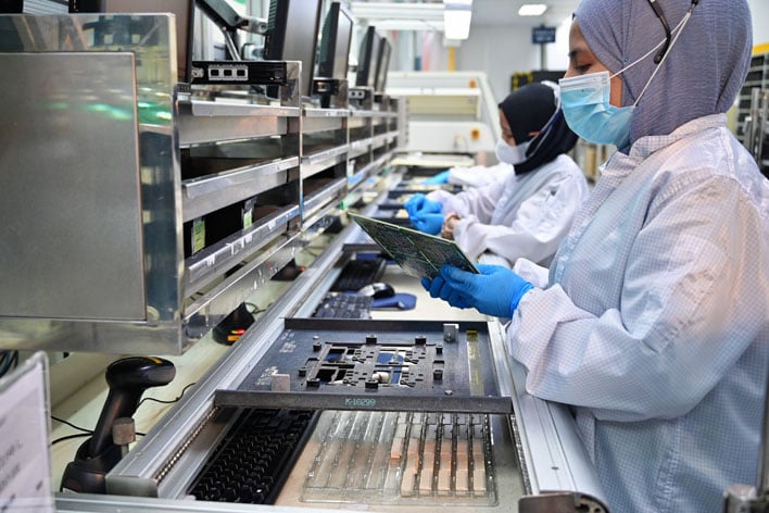
Intel manufactures its own purpose-built PCBs. A majority of this process is automated according to its representatives, but we still saw dozens of stations for workers to hand place components and solder as needed.
Wherever possible, equipment is built to flexibly cover as broad a range of products as possible. In many cases, equipment can be built to accommodate a range of CPU sockets, for example, while some testers will be made with multiple different sockets at the outset so it can freely accommodate any product that comes its way in the queue.
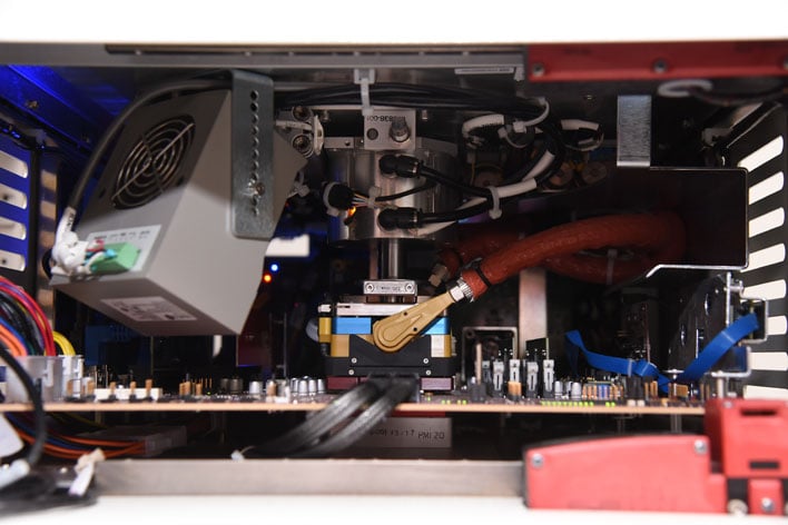
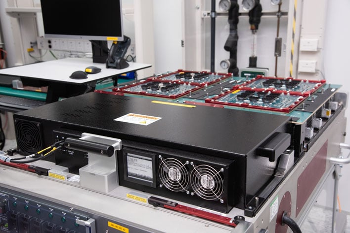
Some of the specific equipment we looked at included the High Density Burn-In (HDBI) Tester, the High Density Modular Tester (HDMT), and the System Level Tester (SLT). The HDBI is built with next-level liquid cooling (perhaps a misnomer on our part) that can precisely control the temperature applied to the package, ranging from sub-zero (C) to north of Tjunc, in addition to coursing voltage.
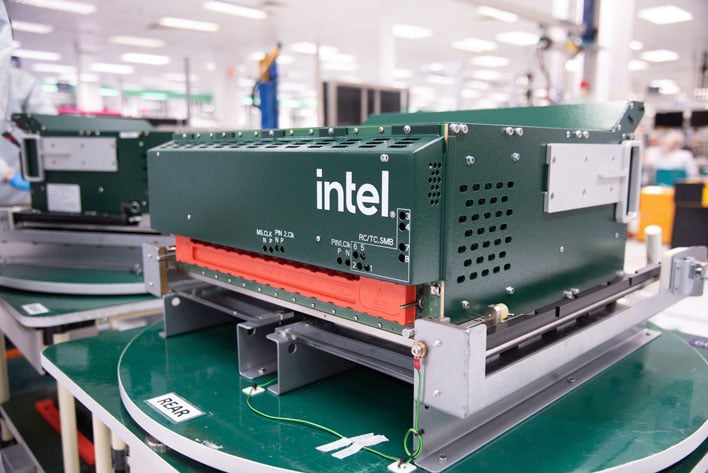
The HDMT is built to provide class or backend testing for Intel’s CPUs. In effect, it joins a board with a CPU-specific socket to a larger green housing via a robust interface. The housing can be outfitted with a series of slot-in cards as needed to test different platform functionalities. In just a few steps, Intel’s engineers can reconfigure the HDMT for a different product or test configuration. The HDMT is used throughout product development and into production ramping.
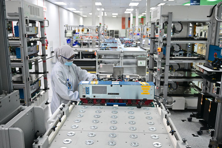
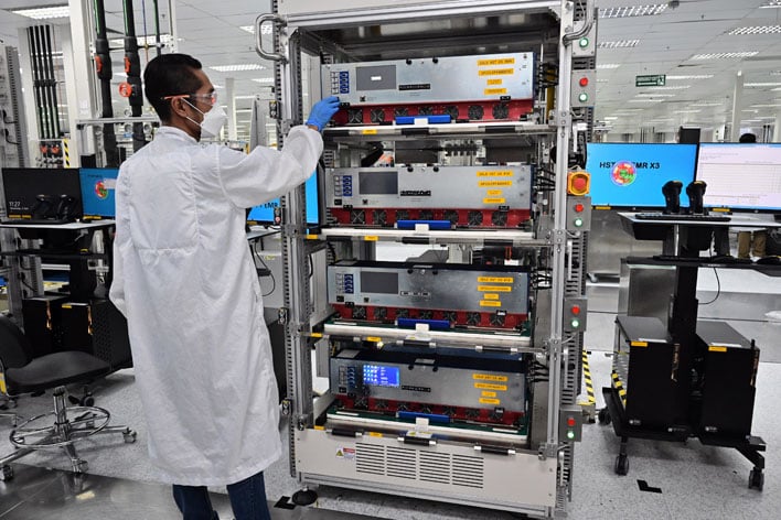
Finally, the SLT is used for Intel’s customer-like testing environment. We were able to see where these are assembled, station-by-station, until the final tester is completed. These are then stacked 4-high in a rack, again to maximize throughput and minimize footprint.
How To Autopsy A Failed Semiconductor Chip
Invariably, some chips will fail during testing at different stages in the manufacturing process. From the earliest silicon samples to ramping high volume manufacturing, semiconductor companies invest a lot into correcting design issues and maximizing yields. Intel’s Failure Analysis Lab (FAL) is equipped with unique tooling to diagnose failures and perform root cause analysis (RCA).
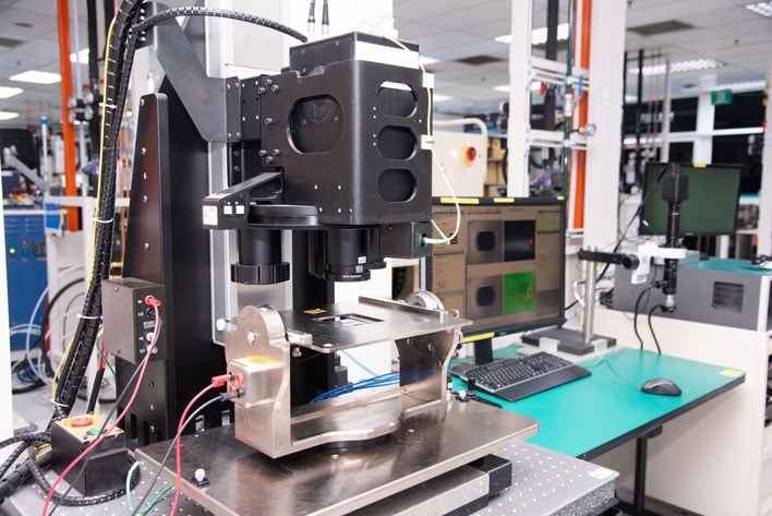
The exact workflow will vary depending on the product and failure, but the goal is to begin as non-destructively as possible. For a completely non-functional chip, this may include microscopic imaging to spot mis-aligned solder balls or ultrasonic scanning of the chip's interior to find imperfections within layers. Elsewhere, the FAL’s workers may apply microprobes to different contacts on the package, then monitor with a thermal camera to identify the location of shorts. Once a failure is located, they may move on to destructive processes, like slicing or grinding.
Other times, an issue may be more subtle. Intel showed us a demonstration of a graphics artifact one sample of a particular chip was exhibiting. It resulted in bright flashes appearing during one part of a scene. With the issue reproduced, the FAL could then work to determine the root cause.
Overall Impressions And Take-Aways From Intel's Malaysia Operations
Despite spending years studying and writing about tech, this was my first time experiencing a semiconductor factory of this size and complexity. What has been most striking is witnessing the scale of operations. We only toured a handful of facilities, and only portions of those facilities at that, but it is still hard to wrap one’s head around just how many chips are being produced there and in other factories like it around the world.
The individual steps, from Die Prep Die Sort to Assembly & Testing, are easy enough to understand. However, the magic comes in making it all flow together as one cohesive machine. There’s enormous complexity in every aspect, from deciding how much of a given product to make (or how much of it can be made), to when that product gets run through a particular machine. Intel is relying heavily on AI and machine learning, not only for QA assessments during the process, but also to guide particular lots of chips through the facilities. It has to account for varying yields as a process matures, instrument wear and tear, physical locations within the facilities, and so much more. Again, Intel’s Malaysia facilities alone are home to nearly a million square feet of manufacturing space.
The stars of the show, though, are Intel’s employees. We met with dozens during our trip, and each expressed genuine excitement and enthusiasm for the job they were performing. Semiconductor companies like Intel don’t exactly open their doors to outsiders like us on a regular basis, and we could tell each was eager to share their work with the world. Of course, the details that could be shared were limited, but we were nonetheless appreciative to learn from true domain experts each step of the way.
We hear a lot from Intel about its IDM 2.0 strategy, and the goals to advance five nodes in four years. It is easy as a skeptical outsider to downplay or dismiss it as some marketing ploy, but it really does appear to be driving Intel’s workforce forward. They are proud of their accomplishments thus far and take the weight of delivering on their goals very seriously.
Whether Intel can continue to march in step and resume industry dominance remains to be seen. The semiconductor industry is unquestionably cutthroat, and we do have to be aware that Intel is carefully showing us its "good side" here. Today’s successes do not guarantee tomorrow’s, but if anyone can get their ducks in a row and weather the storm, it is Chipzilla. The company has done it before, and with the right leadership in place it can do it again.

