AMD Radeon R9 285 GPU Review: Tonga Arrives
AMD Tonga GPU: New Features
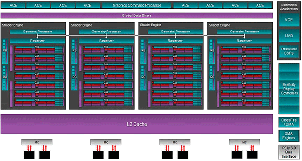
Below we have a block diagram of AMD’s new Tonga GPU. The chip is fabricated on TSMC’s 28nm process node and features approximately 5 billion transistors. The die size is about 359mm2, which is ever so slightly smaller than Tahiti’s 365mm2, even though Tonga packs in about 700 million more transistors. If you recall, Tahiti is the GPU that powers the Radeon HD 7900 series and R9 280 and R9 280X.
Why would AMD release a new GPU that’s roughly the same size and falls in the same class as its predecessors? Because AMD has incorporated some new technologies into this chip that enhance graphics processing and video performance, and more efficiently utilize memory bandwidth.
As it is implements on the Radeon R9 285, the Tonga CPU has 1792 stream processors arranged in 28 compute units, with 112 texture units, and 32 ROPs. And the memory interface is 256-bits wide. At reference clocks, the Radeon R9 285 offers up to 3.29 TFLOPS of compute performance, with a texture fill-rate of 102.8GT/s and a pixel fill-rate of 29.8GP/s. But the Tonga GPU actually features a total of 32 compute units and 2048 stream processors. And there’s speculation that the chip may have the capability to support a 384-bit memory interface. The moral of the story is that while the Radeon R9 285 may be the first graphics card powered by Tonga, it likely won’t be the most powerful. A full implementation of Tonga will probably arrive at some point, perhaps after NVIDIA shows its next hand.
Versus the Radeon R9 280, the Radeon R9 285 offers vastly improved geometry and tessellation performance. The R9 285 can process four primitives per clock cycle and has roughly 2 – 4x the tessellation performance of the R9 280. These enhancements come by way of a more potent front end that is similar to the Hawaii GPU used in the Radeon R9 290 series.
The Tonga GPU used on the Radeon R9 285 has also gained a few new instructions. There are new 16-bit integer and floating point instructions that offer low-power GPU-compute and media processing, SIMD lanes can share data thanks to some new parallel processing instructions, and the task scheduler has also been improved.
Perhaps the biggest change to Tonga in support for a new, lossless color compression technology. AMD is claiming up to 40% higher memory bandwidth efficiency with Tonga. The GPU stores frame buffer color data in this new compressed format, and can read from and write to the compressed data. Though The R9 285’s 256-bit memory interface may seem like a downgrade versus Tahiti’s 384-bit interface, the higher clocks and more efficient utilization of available bandwidth should offset the differences in actual bandwidth somewhat.
Tonga also has an updated video engine which features a higher quality scaler unit. There’s a new pre-scaler that improves the quality of high ratio downscaled media and the chip can upscale / downscale to 4K in real time.
Tonga also gains the updated PowerTune architecture that arrived with the R9 290 series. Previously, a pre-determined power target was used to determine the peak boost clocks of a GPU. If a given workload wasn’t fully utilizing available board power and environmental conditions and temperatures were acceptable, the GPU’s voltage and frequency would be boosted to take advantage of any spare power. The new PowerTune features work in a similar manner, but in lieu of a strict power target they use actual GPU temperature and power targets in their determination of peak boost frequencies and voltages.


