Intel Core M Broadwell Architecture Preview
14nm: It's All In The FinFET
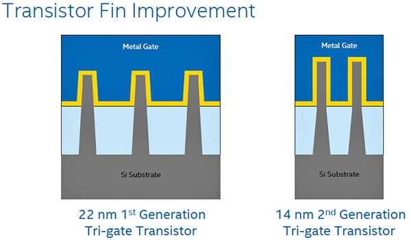
Intel's new 14nm manufacturing process technology for Broadwell is now in volume production and will eventually span Intel's product stack from top to bottom, from the high-end to ultra-low power devices. The technology is based on a tighter transistor fin pitch that extends the height of the SOI (Silicon On Insulator) FinFet designs and tightens the pitch (spacing between fins) from 60nm to 42nm. This allows Intel to pack more transistors into less silicon area with fewer fins and less gate material around them.


However, to be clear, Intel's FinFet technology is unique in that it is based on a "3D Tri-Gate" design that Intel pioneered with their previous generation 22nm process back in 2011. In addition, the benefits of Intel's move to 14nm extend throughout Broadwell's design, to tighter interconnect pitch and gate pitch as well. At 14nm, the advancements we'll step through for Broadwell, are part of how Intel is keeping Moore's Law alive and well.

In terms of major functional blocks, for example, Intel is now able to build SRAM memory cells (used in CPU L2 and L3 cache), in nearly half the area of the previous generation 22nm process. This is a huge gain as memory structures tend to be large consumers of silicon real estate in any design. Broadwell-Y devices (Intel's lowest power 3.5 - 4.5W TDP chip) will have 2MB of shared L3 cache per core (4MB total), which indicates an increase in this resource versus previous generation low-power Haswell chips, which typically have 1.5MB of L3 cache per core (3MB total for low power dual-core Haswell variants). To be clear, some higher-end 15 Watt Haswell dual-core variants do have a full 4MB shared L3 cache. However, remember, Broadwell-Y was targeted for "fanless" designs at a 3.5 - 4.5 Watt TDP (Thermal Design Power) and it still has a full 4MB complement in its dual-core variant. Incidentally, Broadwell also has a larger L2 TLB (Translation Look-aside Buffer), increased to 1.5K from 1K in Haswell. The additional fast, local memory means one thing--more performance--though we'll discuss what to expect in general from Broadwell, shortly.

Intel is claiming that Broadwell-Y offers a greater than 2X improvement in performance-per-watt metrics over the previous generation product. Typically, the company claims a 1.6X improvement in this metric but with Broadwell's better than normal 14nm area scaling per transistor, power consumption and cost per transistor are further optimized. Intel also made some smaller tweaks in the architecture to further optimize Cdyn, or Dynamic Capacitance of processor cores as they respond to workload. In addition, Intel is projecting this same trend of these benefits for their next generation 10nm process node as well.
Finally, though Intel's 22nm process is currently offering Intel's highest yield/lowest defect density per-wafer, the company claims 14nm is quickly on track to line up similarly. When OEM partners begin shipping product in Q4 2014, Intel will have the 14nm process within healthy, nominal limits for large scale volume production.
But enough of this deep-dive silicon geek-out, let's look at what Broadwell-Y will bring to the table, at least from what Intel has disclosed thus far.


