AMD Kaveri Update: A10-7800 APU Review
Introduction and Specifications
AMD updated its family of Kaveri-based A-Series APUs for desktop systems today. We first took an official look at Kaveri back in January, when we evaluated the A8-7600 APU. That particular APU is being re-launched today at a new price point, but AMD is also introducing a couple of new APUs as well, namely the A10-7800 and the A6-7400K. As their names suggest, the A10-7800 is a somewhat higher-end APU than the A8-7600 we initially evaluated, and the A6-7400K is a lower-end variant with fewer cores.

The Updated AMD Kaveri-Based APU Line Up - Find Them At Amazon
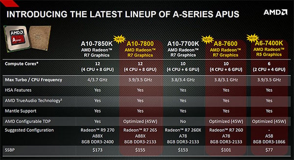
The complete breakdown of AMD’s updated A-Series APU line-up is listed for you here. As you can see, the A10-7800 has 12 total compute core—4 CPU and 8 GPU cores—with average and maximum turbo clock speeds of 3.5GHz and 3.9GHz, respectively. The A6-7400K arrives with 6 total cores (2CPU, 4 GPU), but with the same frequencies. All of the Kaveri-based APUs launching today have configurable TDPs, and support for AMD proprietary technologies like TrueAudio and Mantle, and they have HSA features as well.
We’ve got an A10-7800 in hand and have run it through an array of benchmark to show you what its performance looks like in comparison to a few competing chips. First up though, let’s get some specifications and background information out of the way...

AMD A-Series APU In Socket FM2+ Flavor
|
| Stream Processors | Up to 512 |
| Core Clock | Up to 3.7/4.0GHz |
| Graphics Clock | Up to 720MHz |
| Memory Support | Up to 2400MHz w/ AMP |
| Typical TDP |
45W, 65W, 95W |
| Chipset Compatibility | A88X, A78, A55 |
| HSA Heterogeneous Computing | Yes |
| AMD TrueAudio Technology | Yes |
| API Support |
DirectX 11.2, Mantle |
| Up to 4 “Steamroller” x86 computing cores
Up to 8 GCN-based GPU cores
HSA Hetereogeneous Computing
|
FM2+ Platform
AMD TrueAudio Technology
Unified Video Decoder and Compression Engine
|
Before we get to the benchmarks, we’ve got some features and specifications to share. As you can see in the table above (and as we’ve detailed many times in the past), Kaveri combines AMD’s latest Steamroller CPU microarchitecture with a GCN-based graphics engine, with up to 512 stream processors. Peak CPU clocks will vary depending on model, but the graphics clock maxes out at 720MHz. These AMD desktop-targeted APUs will carry configurable TDPs of 45W – 95W.

AMD’s goal with Kaveri was to target virtually every market segment, from micro-servers all the way on up to high-end desktops. The architecture was designed with performance-per-watt in mind and some SKUs (like the A10-7800 we’ll be showing you here) offer scalable TDPs. The A10-7800 can actually be configured to operate with 45w or 65w TDPs (or any wattage in between with the right motherboard).
Above is a funky Kaveri “die shot” that looks somewhat like a cross between a die map and blurred actual die shot. Regardless, it illustrates where all of the major chip components reside on the APU. Roughly 47% of Kaveri’s die (the large, orange/copper looking block) is dedicated to its GPU. Along the top of this image are the chip's PCI Express and display interface blocks, at the bottom (and the spike about in the middle) is the DDR3 phy and UNB, and to the right are the dual, dual-core X86 Steamroller CPU modules.
All told, Kaveri is comprised of approximately 2.41 billion transistors and has a die size of 245mm2. That’s about a billion more transistors than Richland, with roughly the same die area. AMD was able to accomplish this feat by working with Global Foundries on a new 28nm SHP manufacturing process, that’s less CPU-optimized but offeres better area utilization for graphics. Using this 28nm SHP process, which employs bulk silicon, forced AMD to sacrifice some CPU frequency at the high-end of the TDP scale, but with better power characteristics at the sweet spot.
Since we've already covered all of the features and architectural details of Kaveri in a previous article, we won't re-hash them all again here. If you'd like more information on Kaveri and AMD's vision for its A-Series APUs, we'd suggest checking out this article.


