SanDisk Announces Sampling of 1Ynm Process Technology
When it comes to raw horsepower within the devices that make our lives tick, it can get pretty nerdy... real fast. Take process technology, for example. Everyone loves speed, but it's companies like SanDisk who care about the nuts and bolts that make our gizmos tick. The company has just announced the commencement of customer sampling of flash memory products based on its industry-leading 1Ynm process technology, which represents its second generation 19 nanometer (nm) manufacturing technology.
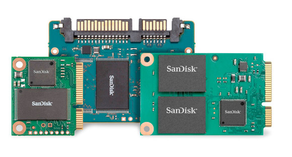
SanDisk’s achievement of this takes its memory cell size from 19nm-by-26nm to 19nm-by-19.5nm, delivering a 25 percent reduction of the memory cell area. SanDisk’s second-generation 19nm memory die uses the most sophisticated flash memory technology node to-date, including advanced process innovations and cell-design solutions. SanDisk's All-Bit-Line (ABL) architecture with proprietary programming algorithms and multi-level data storage management schemes help yield multi-level cell (MLC) NAND flash memory chips that do not sacrifice performance or reliability. In addition, SanDisk’s three bits per cell X3 technology, implemented in the second-generation 19nm node will deliver the lowest-cost flash solutions to address multiple growing end-markets for flash memory.
Soon, this will lead to more memory in tighter spaces, and faster speeds with less surface area. In other words, it's progress like this that'll keep our ever-smaller gadgets from getting slow and cludgy.