Samsung Roadmap Plots Course To Mass Produce 1.4nm Chips In The Near Future
Samsung has shared a new foundry services roadmap, plotting a course from its existing 3nm technology, through 2nm, to 1.4nm semiconductor mass production. According to the South Korean tech giant, these significant steps will take place over the next five years.
Samsung started mass production 3nm mass production at its newest fabs during the summer, in an impressive first for the semiconductor industry. Fierce rivals TSMC are purportedly going to catch up soon, but we haven’t had word of it kick-starting its ‘N3’ mass production as yet.
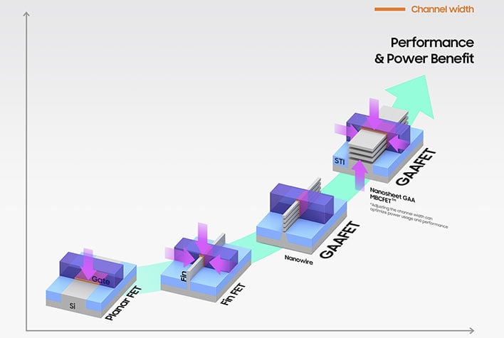
The transition to gate-all-around (GAA) transistor based technology is another advantage Samsung is now enjoying as the first-mover. It was thought this step could have delayed its advance from 5nm to 3nm mass production, but Samsung engineers have ably left this tech hurdle behind them. TSMC, Intel, and others still have work to do to graduate from FinFET transistors – but they will need to embrace GAA for advances in power, performance, and area that the change delivers.
Looking towards the next step for its Foundry Business, in 2025, Samsung says that 2nm will feature an enhanced version of the GAA technology which debuted this summer with its 3nm output. Advancements will continue with the arrival of its 1.4nm process, in 2027. Moreover, other synergistic technological progress is being worked on for Samsung’s upcoming ranges of semiconductor offerings, namely; the development of 2.5D/3D heterogeneous integration packaging technology, 3D packaging X-Cube with micro-bump interconnection, and more.
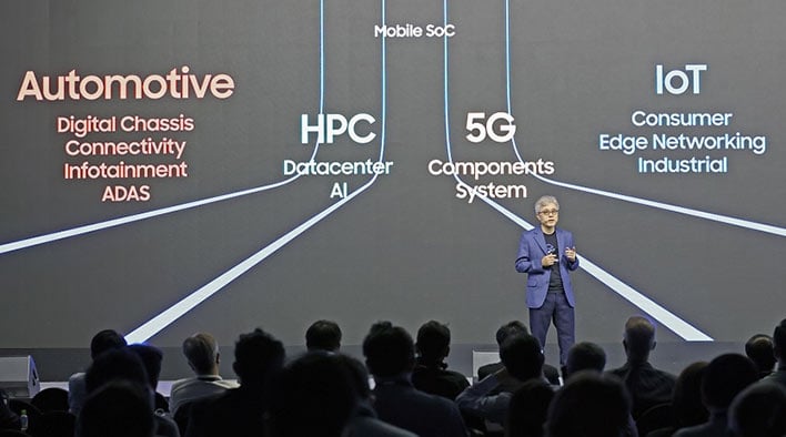
Like TSMC, Samsung has a wide variety of customers, which have helped it stay confident in the face of the widely reported consumer downturn. We have written articles on the less than ideal situations facing a range of consumer PC products, from graphics cards, to memory, to storage. However, foundries are still benefitting from strong demand from segments such as high-performance computing (HPC), artificial intelligence (AI), 5/6G connectivity, and automotive.