Display Material Breakthrough Could Finally Make OLED TVs Cheap And Affordable
A breakthrough at Pusan National University in Korea could hold the key to the large-scale fabrication of high-quality OLED monitors using a solution-processed method. Why is this an important discovery? The researchers behind the project explain that this is a far more economical and less labor-intensive process than the current multi-layer vacuum deposition OLED production method. Moreover, there may be some further benefits to panel efficiency and durability.
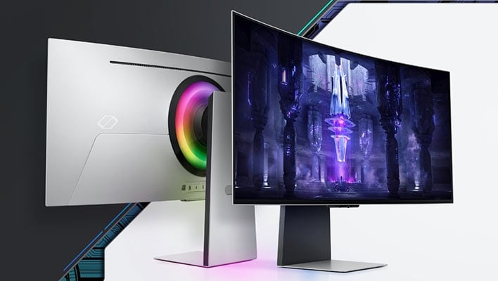
OLED TVs and monitors are undoubtedly attractive, with their stunning contrast ratios, super-fast response times, and great text readability. However, large scale adoption of OLED displays is held back by their relative expense – as we are sure regular readers are well aware. If you look at 34-inch WQHD gaming monitors on Amazon, for example, you will quickly see that those sporting OLED display panels are double the price of the most expensive LCD IPS brethren and triple the price of other lesser featured models.
This scientific research breakthrough was inspired by the latent demand for cheaper OLED displays, and it has been suspected that commercialization of solution-processable panels would be the key to boosting the industry. There were issues with the preparation of the multilayered thin films getting damaged by the necessary solvents in previous attempts to use a solution-processed method. This damage limited the efficiency and shortened the lifespans of solution-processed OLEDs.
The research paper, succinctly dubbed “Synthesis and characterization of thermally cross-linkable poly(iminoarylene) - based hole injection layer for solution-processed organic light-emitting diodes,” reveals the key innovation was the novel material. Thanks to this innovation, a heat-treated construction layer with over 99% solvent resistance was created, with a highly acceptable optimum energy level for its intended purpose, as well as excellent film-forming properties. Overall, the new material was judged to have all the right properties for commercial solution-processed OLEDs.

According to the researchers, previous solution-processed OLEDs showed limited efficiency and short life spans due to the difficulty in stacking the constituent layers. Happily, the new process can stack materials with more finesse thanks to their high mobility – an essential property for accurately constructing the delicate layers of an OLED display panel – the anode, cathode, hole injection layer (HIL), hole transport layer (HTL), etc.