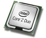
Intel Core 2 Duo E6750 Performance And Overclocking
Introduction and Related Information


Over the last year or so, since Intel's Core microarchitecture and Conroe core were ready to be unveiled at the Intel Developers Forum in early March '06, Intel has been more open and has allowed the media a view into more details regarding upcoming products much earlier than they had before. You don't have to take our word for it, however. Simply look around at all of the early performance previews out of IDF, and the steady flow of announcements regarding Intel's 45nm manufacturing process, metal gate transistors, the Terascale project, Larrabee, Penryn, Nehalem, and a number of other projects, and it becomes readily apparent that Intel wants to get the word out regarding their future products early and often.
Today's news falls into the category of an early announcement as well; a sneak peek, so to speak. In the coming weeks - sometime later this summer - Intel will be officially launching a whole line of desktop processors that feature 1333MHz front side bus frequencies, which is a healthy boost from the current desktop standard of 1066MHz. We've actually got one of these new 1333MHz FSB-equipped chips in house, the Core 2 Duo E6750, and while we can't disclose all of the details regarding this processor just yet, we can talk about its performance and overclockability. And that's is exactly what we're going to do here today, but first let's get some of the particulars out of the way.
|
|
|
We've posted a wealth of information related to Intel's Core microarchitecture and Core 2 Duo and Extreme family of processors here at HotHardware.com. For more background on the technologies employed by the Core microarchitecture and Intel's platform as a whole, we suggest taking a look at few of these related articles. They contain detailed explanations of some of the features common to Intel's legacy products, compatible chipsets, and the new Core 2 Duo and Core 2 Extreme processors:
- Core 2 Extreme QX6800 Review
- Intel P35 Bearlake Chipset
- Core 2 Extreme QX6700 IDF Preview
- Core 2 Duo E6700 & Extreme X6800 Evaluation
- AMD Athlon 64 X2 6000+ (AMD's most recent competitive launch)
- Pentium Extreme Edition 955 & i975X Express Chipset Evaluation
- Pentium Extreme Edition 840 Preview
- Pentium D 820 & i945G/P Evaluation
We cover some specifics regarding Intel's 65nm manufacturing process in our 955XE / i975X evaluation and outline Intel's AMT (Active Management Technology) and IVT (Intel Virtualization Technology), among other things inherent to the Core microarchitecture, in our Core 2 Duo E6700 & Extreme X6800 Evaluation . The other articles listed above will also give you some background as to how the Core 2 has matured, leading up to today.
Beyond the increase in FSB speed, there really isn't too much more to know about the E6750, other than the fact that the chip is based on a new stepping and revision of the Conroe core and that it will require a motherboard and chipset capable of supporting the new 1333MHz FSB, i.e. Intel Bearlake (P3x, G3x) or NVIDIA's nForce 6.


