NVIDIA GeForce GTX 650 Ti BOOST Review
Introduction and Specifications
In the final analysis of our AMD Radeon HD 7790 review, which launched last week, we mentioned that the mainstream GPU landscape would likely change again by the time the 7790 was actually available on store shelves. Although we posted a full review of the card on March 22, they aren’t slated to go on sale until April 2.
Today we're making it clear why we made that statement about the changing GPU landscape. To counter the just-announced Radeon HD 7790, NVIDIA is already launching a new card of its own, which is somewhat of a cross between the GeForce GTX 650 Ti and GeForce GTX 660. The new GeForce GTX 650 Ti BOOST that we’ll be showing you here today takes the CUDA core and texture unit configuration of the GTX 650 Ti and the memory controller and ROP configuration of the GTX 660 and melds them together on a new product that drops in right between the two in NVIDIA’s current GPU lineup.
NVIDIA is also doing some rejiggering of its price structure, which makes the company’s entire mid-range lineup more affordable. Take a peek at the new GeForce GTX 650 Ti BOOST and its specifications and features below, and then we’ll dig in with a closer look at a retail-ready version from EVGA and some benchmarks...

NVIDIA GeForce GTX 650 Ti BOOST
|
| Processing Units | |
| Graphics Processing Clusters | 2 or 3 |
| SMXs | 4 |
| CUDA Cores | 768 |
| Texture Units | 64 |
| ROP Units | 24 |
| Clock Speeds | |
| Base Clock | 980 MHz |
| Boost Clock | 1033 MHz |
| Memory Clock (Data Rate) | 6008 MHz |
| L2 Cache Size | 384 KB |
| Memory | |
| Total Video Memory | 2048MB |
| Memory Interface | 192-bit |
| Total Memory Bandwidth | 144.2 GB/s |
| Texture Filtering Rate (Bilinear) | 62.7 GigaTexels/sec |
| Physical & Thermal | |
| Fabrication Process | 28 nm |
| Transistor Count | 2.54 Billion |
| Connectors | 2 x Dual-Link DVI, 1 x Mini HDMI |
| Form Factor | Dual Slot |
| Power Connectors | 1 x 6-pin |
| Recommended Power Supply | 450 watts |
| Thermal Design Power (TDP) | 134 watts |
| Thermal Threshold | 98° C |

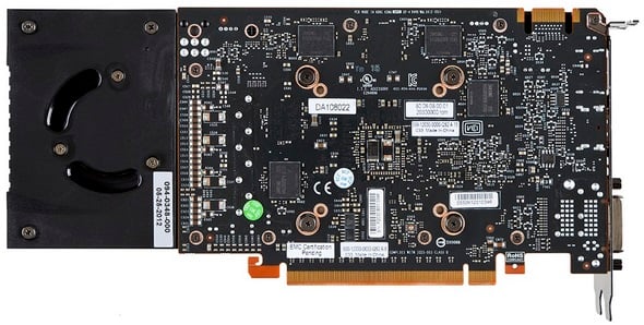
NVIDIA GeForce GTX 650 Ti BOOST PCB View
Like the GeForce GTX 660 and the GTX 650 Ti that came before it, the new GeForce GTX 650 Ti BOOST is based on NVIDIA's GK106 GPU. Although the GK106 features all of the same technology as NVIDIA’s more powerful Kepler-based graphics processors, like the GK104, the GK106 is somewhat smaller and scaled-down versus its higher-end counterparts.
Above is a list of the GK106's main features and specifications, as the chip is configured on the GeForce GTX 650 Ti BOOST. As you can see, the GK106 is manufactured using TSMC’s 28nm process node and it is comprised of approximately 2.54 billion transistors. The GPU features two or three Graphics Processing Clusters (GPC) with four SMXs and a total of 768 CUDA cores. There are also 64 texture units and 24 ROPs within the GPU, along with 384K of L2 cache. Memory is linked to the GPU via a 192-bit memory interface.
In comparison to the GeForce GTX 660, the new 650 Ti BOOST has a similar memory interface and cache configuration but with fewer CUDA cores and texture units, which results in lower compute performance and fillrate but similar memory bandwidth.
NVIDIA’s reference specifications call for a base GPU clock of 980MHz on the GeForce GTX 650 Ti BOOST, with a boost clock of 1033MHz and a memory clock of 1502MHz (6008MHz effective). At those frequencies, the GeForce GTX 650 Ti BOOST will offer up to 144.2GB/s of memory bandwidth and 62.7GTexes/s of textured fillrate. Many of NVIDIA’s partners, however, are ready with factory-overclocked models (one of which we’ll show you on the next page) that will offer somewhat higher performance characteristics.
The GeForce GTX 650 Ti BOOST has a TDP of 134 watts and requires a single supplemental 6-pin PCI express power feed. Cards are two slots wide but sport a short PCB, like the GeForce GTX 660 Ti and some GeForce GTX 670 cards. The output configuration is the same 2 x Dual-Link DVI, 1 x mini-DP, and 1 x HDMI setup as the GeForce GTX 650 / 660 Ti, as well.


