Intel 45nm Fab Process And Penryn Preview
The Penryn Die and New Fabs
![]()
Today's announcement isn't about a breakthrough that won't bear fruit for many years. The first products produced with the new high-k and metal gate transistors will be available in just a few months and Intel plans to ramp up production in three new fabs over the next year or so.
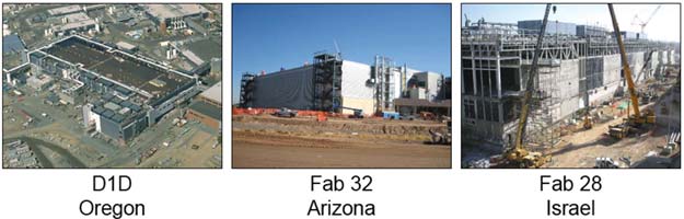
Intel's D1D Oregon fab will be the first, and it is where current sample were developed. Fab 32 in Arizona will come on-line a few weeks later and begin manufacturing 45nm high-k and metal gate products in the second half of this year, and Fab 28 will come on-line in Israel sometime in 2008, if all goes according to plan. In total, when all is said and done, Intel will have three 45nm fabs by the end of next year at an investment of about $9 billion. Between the three facilities, they'll have about a 1/2 million square feet of clean room.
;)
;)
As we've mentioned, today's announcement by Intel is already very real. The images above show an engineer holding a 300mm wafer of SRAM dice produced at 45nm, and the image on the right is a die-shot of an upcoming processor in the Core 2 family, currently code-named "Penryn". Penryn will bring with it microacrchitectural improvements over Conroe (current Core 2 product), larger cache sizes, and SSE4 support. Also, although clock speeds will be increased, processors based on Penryn should fall within the same thermal envelopes as Conroe.
Intel said the first products to use this technology will likely be 35W mobile CPUs, with servers and desktops to follow depending on platform readiness. If your wondering if your motherboard will support Penryn, Intel expects some motherboard developers will have to make minor modification to support Penryn, which include some BIOS changes and perhaps electrical changes. Some of the current crop of LGA775 compatible motherboards are likely to work, however. It'll be a similar situation to the Conroe launch.
We should also note that Intel has already showcased working Penryn processors in action. At a press event on January 25, 2007, presenters Mark Bohr and Stephen L. Smith showcased Penryn in the following five configurations:
- 45nm dual core mobile processor in a notebook with Microsoft Vista running Microsoft Office 2003 applications
- 2.13GHz 45nm dual-core desktop processor running high definition video content (1080P) under Microsoft Vista.
- 1.86GHz 45nm quad-core desktop processor running Ubisoft's Rainbow Six Las Vegas game under Microsoft Vista
- Two, 2.13GHz 45nm dual-core processors running Glaze* Workstation application under Microsoft Windows 2000 Advanced Server
- Two, 2.13GHz 45nm quad-core processors encoding a video in Adobe Premier under Microsoft Vista
So, what does all this mean to you and me? Basically, it means Intel is poised and ready to produce next-generation 45nm processors using high-k and metal gate transistors. And also those processors will be more economical to produce, will require less power, generate less heat, and run at higher frequencies than Intel's current 65nm products, which are already the most advanced in the industry. This is a show of strength if you will, and an impressive one at that. How impressive? We'll wrap-up here with a few quotes from Gordon Moore (Intel), Professor Dimitri Antoniadis (MIT), and Yoshio Nishi (Stanford) telling you what they think of Intel's achievements.
|
"The implementation of high-k and metal gate materials marks the biggest change in transistor technology since the introduction of polysilicongate MOS transistors in the late 1960s" - Gordon Moore "The Intel 45-nm CMOS technology marks a historic milestone for the semiconductor industry. Similar to the transition from single metal (Al) gate to polysilicon gate that has allowed optimal nFET and pFET design, the introduction of dual metal with high-k-insulator gate-stack opens the path for optimal design of both types of FETs, at insulator thicknesses necessary for continuing device scaling that are impossible to reach with the industry-standard silicon-dioxide-based insulators. Many options of high-k gate-stacks have been the target of intense industry and academic research for many years now, but Intel's demonstration of a manufacturable dual-metal/high-k solution is a remarkable first." - Prof. Dimitri Antoniadis "It is a huge break through to replace more than three decade's long successful polysilicon gate technology with a new high-k+metal gate technology. Though the combination of high-k dielectrics and metal gate electrode for advanced CMOS has been extensively studied by many researchers around the world as the ideal MOS gate structure, the technical hurdle to bring the technology to manufacturing floor has been believed still too high for the 45nm node. As a researcher in this field, I am pleasantly surprised by the announcement and would like to congratulate Intel researchers for their success that Intel has demonstrated 45nm microprocessors with their high-k and metal gate technology. Even though specific metal and high-k material have not been disclosed at this moment, this is a revolutionary step toward the world of sub-50nm CMOS integrated circuits, as this new technology will drastically improve transistor performance in all fronts of electrical specifications, resulting in significant improvement of IC performance." - Yoshio Nishi |
Discuss This Article In HotHardware's PC Hardware Forum


